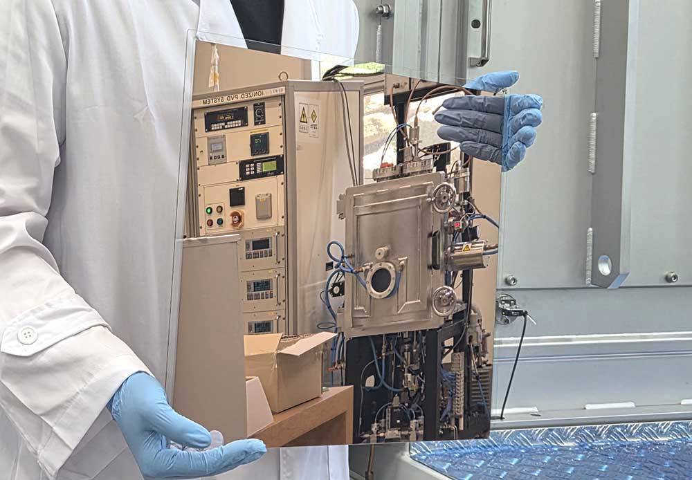
CIT CopperFlat PackageCore / Source=CIT
With the activation of AI, there is a growing need for next-generation material technology that combines high performance, low power consumption, and eco-friendliness to process large volumes of data quickly. In particular, the development of next-generation materials for AI semiconductors is being highlighted as a key to industrial competitiveness. Amid this trend, domestic startups are also focusing on developing next-generation materials using proprietary technology. A representative company is CIT (Copper Innovation Technologies).
Established in 2023, the advanced material technology startup CIT recently introduced the planar copper deposition glass substrate 'CopperFlat PackageCore (CuFlat-PKGCore)'. This product is a glass substrate for next-generation semiconductor packages with copper deposited thinly and flatly. Through this, CIT won the Innovation Award at the Future Innovation Technology Expo (FIX) 2025 and the Innovation Award at the International Consumer Electronics Show (CES) 2026. CIT plans to accelerate its entry into the global market based on these achievements.
CIT's ASE technology combining insulator and copper in a single-crystal structure / Source=CIT
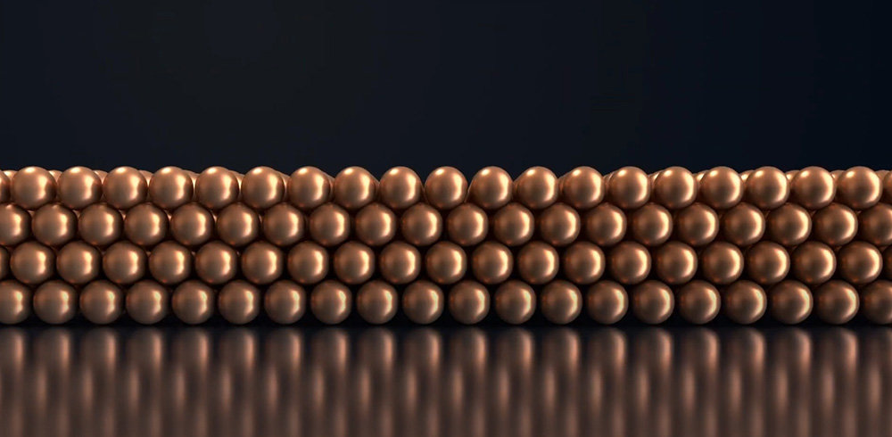
Proprietary ASE Technology Recognized by International Academic JournalsCIT's core technology is 'ASE (Atomic Sputtering Epitaxy)' technology. ASE technology is a molecular bonding technology that thinly coats copper on an insulator. CIT uses ASE technology to combine the insulator and copper in a single-crystal structure. Since no separate adhesive is used, the surface is uniform and stable enough not to fall off even when heat is applied. The ability to stack copper atoms layer by layer allows precise control of thin film thickness at the nanometer (nm) level, which is also an advantage of ASE technology. Through this, CIT succeeded in implementing a planar copper surface of 3nm or less.
ASE technology has been officially recognized by academia. It was published in the world-renowned scientific journal Nature in May 2022 and was also introduced in the prestigious international journal in the field of materials engineering, Advanced Materials. These journals are known for their rigorous review processes and are recognized for their high credibility, influence, and authority in academia.
CIT is developing solutions that can be applied to various industrial fields, such as high-frequency communication equipment, transparent antennas, and displays, using ASE technology. Recently, it also introduced the CopperFlat PackageCore, a copper deposition glass substrate for semiconductor packages.
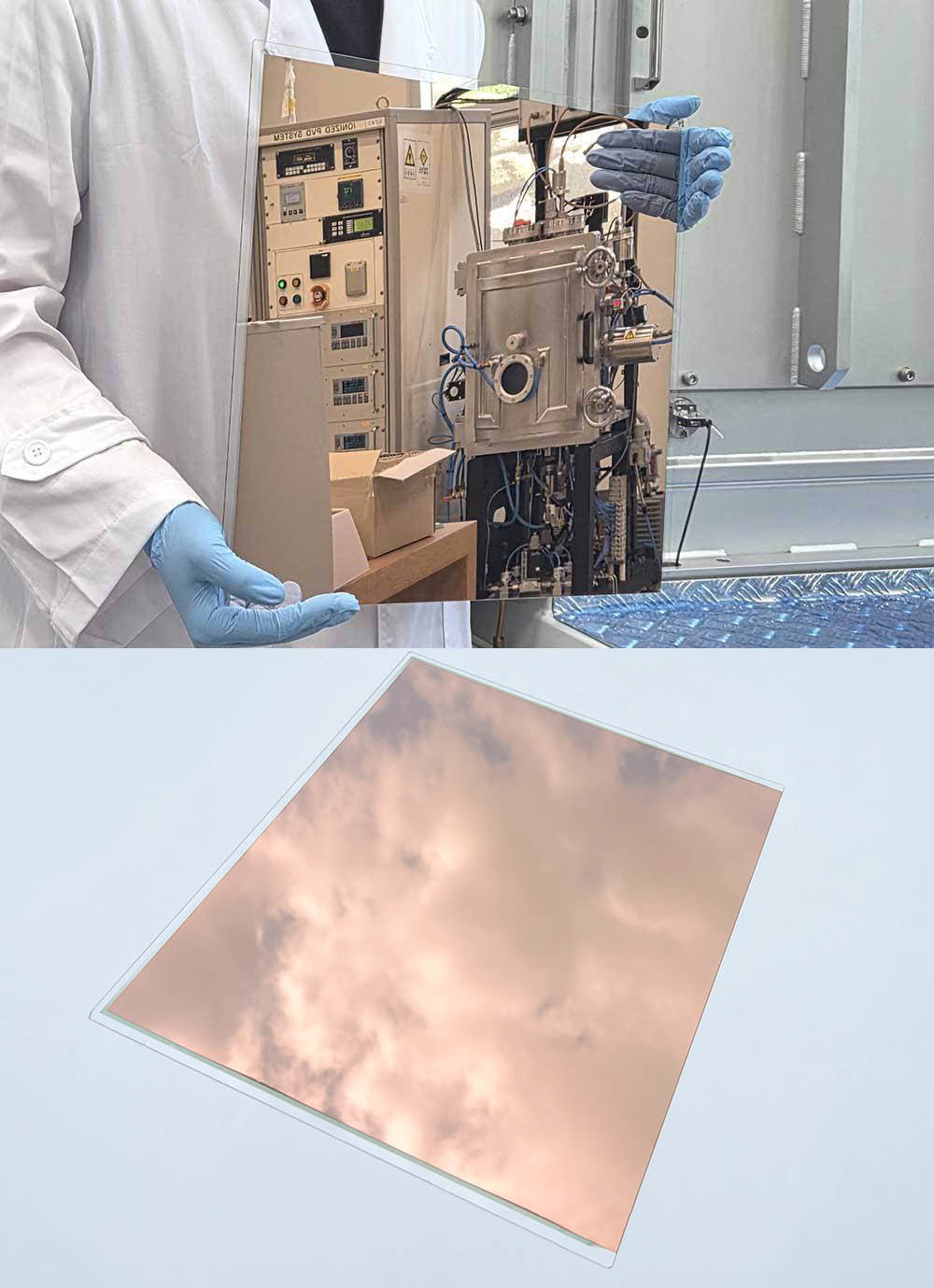
Package Substrate for Next-Generation Semiconductors, CopperFlat PackageCoreThe CopperFlat PackageCore is a product that deposits copper thinly and flatly on a glass substrate, which is gaining attention as a material for next-generation semiconductor package substrates.
The most significant feature is its surface roughness. CIT implemented the surface roughness of the CopperFlat PackageCore to be 3nm or less. This is more than 200 times lower than the roughness of the current material used for semiconductor package substrates for AI accelerators, HVLP4 copper foil. As a result, high-frequency signal loss and power consumption are reduced, enabling fast and stable data transmission. The freedom of substrate design is also enhanced, allowing the design intent of semiconductor package engineers to be fully reflected.
CopperFlat PackageCore developed by CIT with ASE technology / Source=CIT
It also has excellent stability in high-temperature environments. While existing copper materials oxidize at 100°C, the CopperFlat PackageCore maintains stability even at 250°C. It operates stably without performance degradation even in semiconductors for AI accelerators with severe heat generation. Additionally, the CopperFlat PackageCore can be applied to various semiconductor package glass substrates, including borosilicate and alkali-free series, as well as core and interposer substrates.
CIT has also realized an eco-friendly manufacturing process. By using pure copper instead of a mixture, material waste is reduced, and process steps are minimized. The process is simplified by eliminating the seed layer deposition and chemical mechanical polishing (CMP), which are essential steps in the existing semiconductor package substrate process for AI accelerators. Since it is not chemical plating, no chemical wastewater is generated. Moreover, by using 100% recycled copper scrap, carbon emissions are reduced by more than 95% compared to existing products.
When the CopperFlat PackageCore is applied to AI-related data centers, energy-saving effects can also be expected. It can operate stably at temperatures about 20°C higher than the recommended operating temperature of existing data centers (18-27°C according to the American Society of Heating, Refrigerating and Air-Conditioning Engineers), significantly reducing the energy and cost required for cooling, such as electricity and water.
CES and FIX Innovation Awards, Accelerating Global Market EntryCIT received innovation awards at domestic and international exhibitions with the CopperFlat PackageCore. In October, it received the 'FIX Innovation Awards' at FIX 2025 held in Daegu, awarded to companies showcasing innovative technology and products.
CIT CopperFlat PackageCore selected for CES 2026 Innovation Award / Source=CES
It was also selected as a CES 2026 Innovation Awards Honoree. The CES Innovation Awards are given by the Consumer Technology Association (CTA), which hosts CES, evaluating technology, completeness, and utility comprehensively before the opening of CES each year. CIT was selected for the innovation award for the second consecutive year following CES 2025.
CIT analyzed that these achievements were the result of recognizing the innovation in the CopperFlat PackageCore's low surface roughness, stability in high-temperature environments, eco-friendly processes, and energy-saving technology.
CIT plans to accelerate its entry into the global market based on the innovation awards received at domestic and international exhibitions. It is currently conducting proof of concept (PoC) for product supply with Japanese glass substrate and transparent antenna manufacturers and American semiconductor equipment companies. Additionally, it is jointly developing AI accelerator substrates with domestic conglomerates, preparing for global market entry. CIT aims to expand the application of ASE deposition technology, focusing on Korea, the United States, Japan, and Taiwan.
Jung Seung, CEO of CIT, stated, “The awards at FIX 2025 and CES 2026 are the result of the recognition of CIT's proprietary ASE technology and the excellent technology of the CopperFlat PackageCore in domestic and international markets,” and expressed his ambition to “present a new standard in the global semiconductor packaging market by simultaneously realizing energy savings and eco-friendly transitions suitable for the AI semiconductor era.”
IT Donga Reporter Han Man-hyuk (mh@itdonga.com)
ⓒ dongA.com. All rights reserved. Reproduction, redistribution, or use for AI training prohibited.
Popular News