HBM alone can't keep up with GPU computing... Focus on HBF with 10 to 100 times capacity
Manufactured by stacking NAND flash in 3D... Overcoming the 100,000 write cycle limit is a challenge
SK Hynix partnered with SanDisk in August... Industry competition over 'HBF standard dominance'
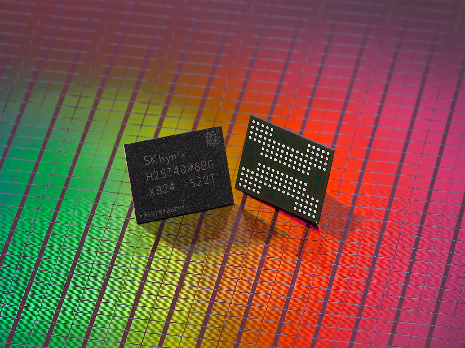
The next-generation AI memory, High Bandwidth Flash (HBF), is a device that stacks larger-capacity NAND Flash in three dimensions, slower than DRAM. It is expected to particularly aid in enhancing AI inference capabilities. Getty Images Korea
As the data handled by Artificial Intelligence (AI) and the scale of AI inference models grow, the need for hardware advancements to support this is also increasing. The emergence of High Bandwidth Memory (HBM), a device suitable for implementing AI technology, has granted domestic semiconductor company SK Hynix a leading position in the memory semiconductor market. HBM is a device made by stacking fast memory semiconductor DRAM in three dimensions.
With evaluations suggesting that HBM alone cannot keep up with the computational speed of GPUs, a new memory semiconductor, High Bandwidth Flash (HBF), was proposed as the next-generation goal starting this summer. HBF is a concept that integrates large-capacity NAND Flash memory, slower than DRAM, by stacking it in three dimensions like HBM, drilling holes, and installing elevator-like connection pathways. In August, SK Hynix and SanDisk joined forces to preempt the HBF standard ahead of competitors like Samsung Electronics.
On the 4th, Professor Kim Jeong-ho of the Department of Electrical and Electronic Engineering at KAIST, met in Daejeon, emphasized, "The current performance of Samsung Electronics and SK Hynix depends on HBM, but in 10 years, it will be determined by HBF." He predicted that "since HBF shares and recycles most of the basic technology and process equipment with HBM, its development speed will be very fast," and anticipated the first appearance of HBF in 2027, with finished products like GPUs equipped with HBF launching in 2028.
● HBM as a Bookshelf, HBF as a Library GPUs are processors specialized for parallel processing calculations, suitable for AI learning or inference. HBM enhances AI performance by quickly exchanging data and computation results needed for GPU calculations. Although HBM emerged due to the limitations of existing memory, even now, the time share of GPU calculations during AI tasks is only about 20-30%, indicating a "bottleneck" in memory. Professor Kim stated, "AI performance is determined by memory," adding, "Even if NVIDIA in the U.S. releases new GPUs, memory innovation is necessary."
HBF is not a substitute for HBM but an additional component. While their roles are similar, they are slightly different. Large data that HBM cannot handle is transmitted from data centers connected via networks. HBF's role is to bring part of the data center closer to the GPU. The GPU exchanges data with HBM, and HBM with HBF. If HBM is likened to a bookshelf for frequently used information, HBF is akin to a library.
Professor Kim explained, "HBF is relatively slower than HBM but has 10 to 100 times the capacity," and noted, "It will particularly aid in inference capabilities rather than AI learning." For HBF to be applied, the software system must also be upgraded to utilize HBF during GPU computations.
● Overcoming NAND Lifespan Challenges… Limited Power Savings NAND operates by applying strong voltage to induce electrons to penetrate a barrier that is usually difficult to cross, trapping them in a space called a "floating gate," and defining information by the presence or absence of electrons. The existing NAND technology naturally develops defects and errors during the 'writing' process of trapping electrons to record information, which is repeated. Unlike DRAM, which has no limit on the number of times it can be written, NAND reaches the end of its lifespan after about 100,000 writes.
Professor Kim stated, "Scientists need to find new materials and structures to solve this issue," and suggested, "A new device with larger capacity than DRAM and capable of operating quickly without a limit on the number of times may emerge."
Half of the personnel in Professor Kim's research lab study HBM, and the other half study HBF. Students approach the research with the perspective that understanding the operating principles of AI is necessary to implement the optimal memory semiconductor structure. Simultaneously, they utilize AI to enhance performance by increasing the connectivity between HBM and GPU and in designing HBF structures.
Regarding the global increase in power consumption due to AI advancement, a fundamental limitation was presented. Even if low-power devices are implemented following the 'Von Neumann architecture,' a computer structure based on silicon material consisting of a computing unit, memory, and program, there are constraints in reducing power consumption.
Professor Kim projected, "If companies providing AI services start releasing essential AI apps for our lives, users may pay in a subscription form to cover power production costs."
ⓒ dongA.com. All rights reserved. Reproduction, redistribution, or use for AI training prohibited.
Popular News